Invented by CHOI; Jung Hwan, YANG; Sung Mo
In this blog, we will break down a new patent about a smarter way to handle data inside hardware accelerators, like those used in artificial intelligence (AI) and neural networks. The goal is to make sense of the technical ideas, explain why they matter, and show you how this invention could change the way hardware devices work. Let’s get started.
Background and Market Context
Imagine your computer or phone trying to learn, think, or see patterns—just like a person. This is what AI, and more specifically neural networks, are all about. These neural networks need a special kind of “helper” called a hardware accelerator. The job of a hardware accelerator is to do math and move lots of numbers very fast. This helps the AI work quickly, saving time and energy.
In recent years, more people want their phones, cars, and smart devices to do things like recognize photos, translate languages, or even drive themselves. To do this, devices need to handle huge amounts of data quickly and use as little power as possible. This is where hardware accelerators come in. They act like super-fast calculators, making sure everything runs smoothly.
But as the data grows, moving it around becomes a big problem. Think of it like trying to pour a huge bucket of marbles through a tiny funnel—it takes more time, and the funnel can get stuck. In computers, the “funnel” is the memory and the way data is organized. If the data is not packed and read in the right way, the hardware accelerator gets slowed down or even stuck. This means your phone or computer might feel slow or use more battery.
Tech companies have been searching for clever ways to handle data better. They want their AI chips to be small, fast, and not waste energy. This is important in phones, cars, and even smart refrigerators. The market for these chips is huge and growing, with more gadgets needing smarter, faster brains.
This patent addresses a big pain point: how to break up data, store it, and read it in a way that never wastes time or space. If you’re a chip designer or a company building AI into your products, this invention matters to you. It promises smoother, faster, and more energy-friendly data handling. That means better user experiences and longer battery life.
Scientific Rationale and Prior Art
To see why this invention is needed, we need to look at how things were done before and the problems with those ways.
Imagine a big table filled with numbers—this table is called an “array.” When an AI chip wants to do its job, it needs to read this table, do some math, and then spit out a new table with the answers. The problem is, the chip can only handle a small part of the table at a time. It’s like trying to read a huge book, but you can only see one page at a time.
Before, the data would just be dumped into the chip in big chunks, not caring about the order. Sometimes, the chip needed the numbers in one order, but the data was given in another. This is like trying to assemble a puzzle, but the pieces come to you out of order. It wastes time because the chip always has to wait for the right piece.
People tried to solve this by dividing the data into groups or “blocks” and using tricks like compression, which is a way to make the data smaller. This helped a bit, but it created new problems. For example, if you make a group too big, you have to wait for the whole group before you can use any of it. If you make the group too small, you waste space and time moving lots of tiny pieces.
Earlier inventions also didn’t pay much attention to the “direction” in which the data is read and written. In a simple table, you can move left to right (rows) or up and down (columns). Sometimes the chip wants to read across the rows, and other times it needs to go down the columns. If you store the data in the wrong order, the chip spends a lot of time jumping around, which is slow.
Another problem is with compression. When you shrink the data, you need to unpack it before you can use it. If the chip only has a small buffer (a tiny storage area), it can’t unpack huge pieces at once. This means the chip might have to wait, making the whole process slow.
In summary, the old ways of handling data were:
– Not flexible with how data is grouped.
– Not smart about the order (direction) of reading and writing.
– Not efficient when unpacking compressed data.
– Wasted precious memory space and slowed down the chip.
This is why the new invention is important. It looks at how to break up and store data in a way that matches how the chip actually wants to use it. It’s like giving the puzzle pieces to the builder in the exact order they need them, so they never have to stop and wait.
Invention Description and Key Innovations
Now, let’s dive into what the patent actually does and why it matters.

The invention is a hardware accelerator, which has a few main parts: a control part, a data operation part, and sometimes special helpers for compression and decompression. The heart of the invention is in how it groups, stores, and reads data.
Here’s the simple idea:
– The data (like a big table or array) is broken into groups.
– These groups can be compressed to save space, or left as they are.
– The way data is stored (which group comes first) can be different from the way it’s read.
– The control part is smart: it figures out what order the data will be needed in, and arranges for it to be read that way.
– The chip never has to wait for a huge group to be ready—it only waits for the part it actually needs.
Let’s break it down even more:
Smart Grouping and Compression
The data isn’t just split randomly. The groups are made so that they fit perfectly into the chip’s buffer. If the buffer can hold four pieces, the groups are made that size. This means the chip never wastes space or time.
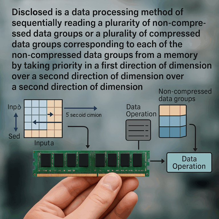
When the data is written to memory, it’s grouped and compressed in one direction (say, row by row). But when the chip needs to read it, it might want to go in the other direction (column by column). The control part knows how the chip will use the data, and it rearranges the reading order to match.
Order and Direction Matter
In this invention, the “direction” isn’t just a detail—it’s the key. The chip might write the data in rows, but later, it might need to read it in columns. The control part keeps track of this and makes sure the right groups are ready at the right time. This is a big improvement over older designs, where the order was fixed and couldn’t match the chip’s needs.

Real-Time, Non-Stop Processing
Because the groups are made to fit the buffers and are prepared in the right order, the chip never has to wait for a big group to unpack before it can start work. As soon as the needed group is ready, it goes to work. This keeps everything moving and makes the most of the chip’s speed.
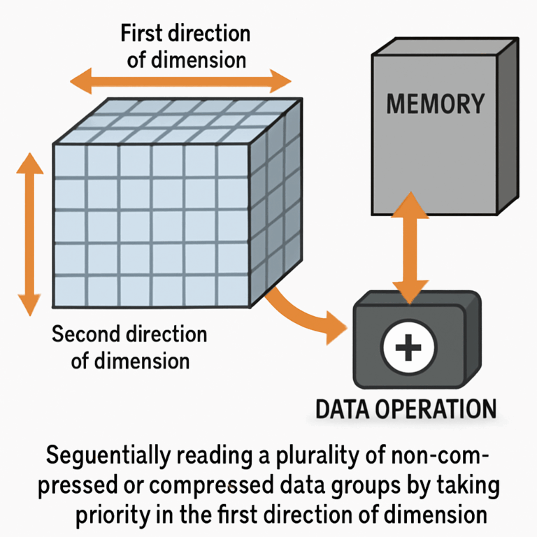
Flexible for Any Size or Shape
The invention isn’t just for two-dimensional tables—it works with three, four, or even more dimensions. No matter how the data is shaped, the control part can figure out the best way to split and read it.
Better Memory Use
Because the groups are matched to the buffer size, there’s no wasted space. The chip can read and write data without needing a giant memory. This makes the chip smaller and uses less power, which is important for phones and small devices.
Compression and Decompression On the Fly
If the data is compressed, the chip has a helper part that unpacks it just in time for use. The control part makes sure only the needed groups are uncompressed, saving time and memory.
Scheduling and Control
The real magic is in the control part. It knows in advance how the data will be used, and it plans the reading and writing to match. This is like having a really good coach who always puts the right player in the right spot at the right time.
Adaptable to Many Devices
This invention isn’t stuck to just one kind of chip or device. It can be used in many different accelerators, from neural networks in phones to smart cameras and even self-driving cars.
Putting It All Together
Here’s how it works in practice:
– The hardware accelerator gets a big chunk of data it needs to process.
– The control part splits the data into groups that match the chip’s buffer size.
– If needed, these groups are compressed to save space.
– The groups are stored in memory in the order that’s best for writing (maybe row by row).
– When the chip is ready to use the data, the control part figures out what order it needs (maybe column by column).
– The needed groups are read, decompressed if necessary, and sent to the chip, just in time for processing.
– The whole process repeats, keeping everything running smoothly.
Because of this smart handling, the chip is always busy, never waiting, and never wasting space. This means faster, more energy-friendly AI for your devices.
Conclusion
This patent brings a thoughtful and simple solution to a hard problem. It helps hardware accelerators handle data in a way that matches exactly how they need it, making the chips work faster and use less energy. By splitting data into the right-sized groups, paying attention to the direction of reading and writing, and using smart control, this invention can make AI chips in phones, cars, and smart devices much better.
If you’re designing AI hardware or care about getting the best performance from your devices, this patent offers a clever path forward. It’s not just about moving data—it’s about moving it the right way, at the right time, every time.
Click here https://ppubs.uspto.gov/pubwebapp/ and search 20250231808.